• Hey, guest user. Hope you're enjoying NeoGAF! Have you considered registering for an account? Come join us and add your take to the daily discourse.

Inside Ratchet and Clank: Rift Apart on PS5: The Insomniac Technology Breakdown

Shmunter

Member
And this:


Anyone still latching on to "well, muh cpu can handle that" is living in a dreamland.

Yeah probably repeating what’s already been covered here…

Even if the most powerful CPU’s were to do it in real-time in parallel while running game code and gfx draw calls. It first needs to load it to ram, decompress back into ram and copy it into vram. Highly inefficient

On PS5 you just request it, and the asset lands in ram decompressed ready to use, super fast, low latency and free of computation resources.

The entire software decompression served its purpose when the data rate was limited by hdd speed. Once you open the tap to nvme speeds, the workload just exponentially increases and cannot be managed during gameplay for streaming.

Its why gfx card manufacturers are proclaiming to do it on GPU to overcome the cpu work and the double handling. Will be curious if it’s successful or just lip service.
 

ratburger

Member
Is it really that severe? If it really is that bad they should have just ate the cost of the cache. Or gone with less cores and more cache.

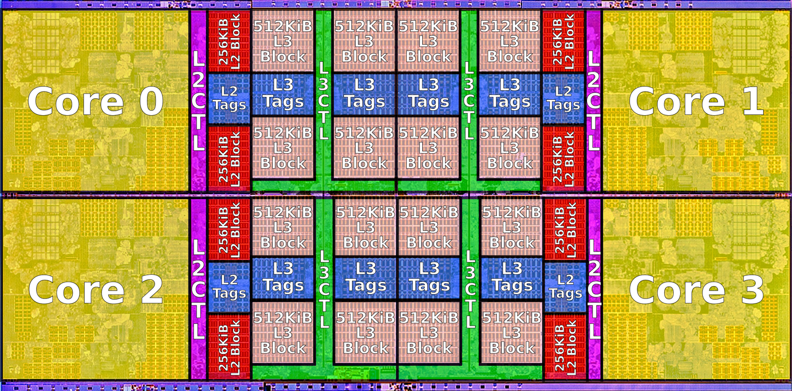
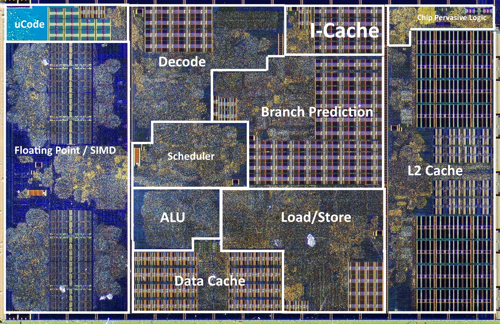
There's a reason a CPU is mostly cache: every cache miss means going out to RAM, during which the core is twiddling its thumbs for hundreds of CPU cycles. If you look at a modern CPU, as little as 10% of it will be devoted ALUs and FPUs. An overwhelming percentage of the transistor budget is devoted to the various caches: L1, L2, L3, instruction.

Zen2 die:
1600px-amd_zen_ccx_2_%28annotated%29.png

source: https://en.wikichip.org/wiki/File:amd_zen_ccx_2_(annotated).png

Zen2 core:
5017e5_982e0e47d7c04dctkcg.jpg

source: https://forums.anandtech.com/threads/annotated-hi-res-core-die-shots-of-zen-1-and-2.2577382/

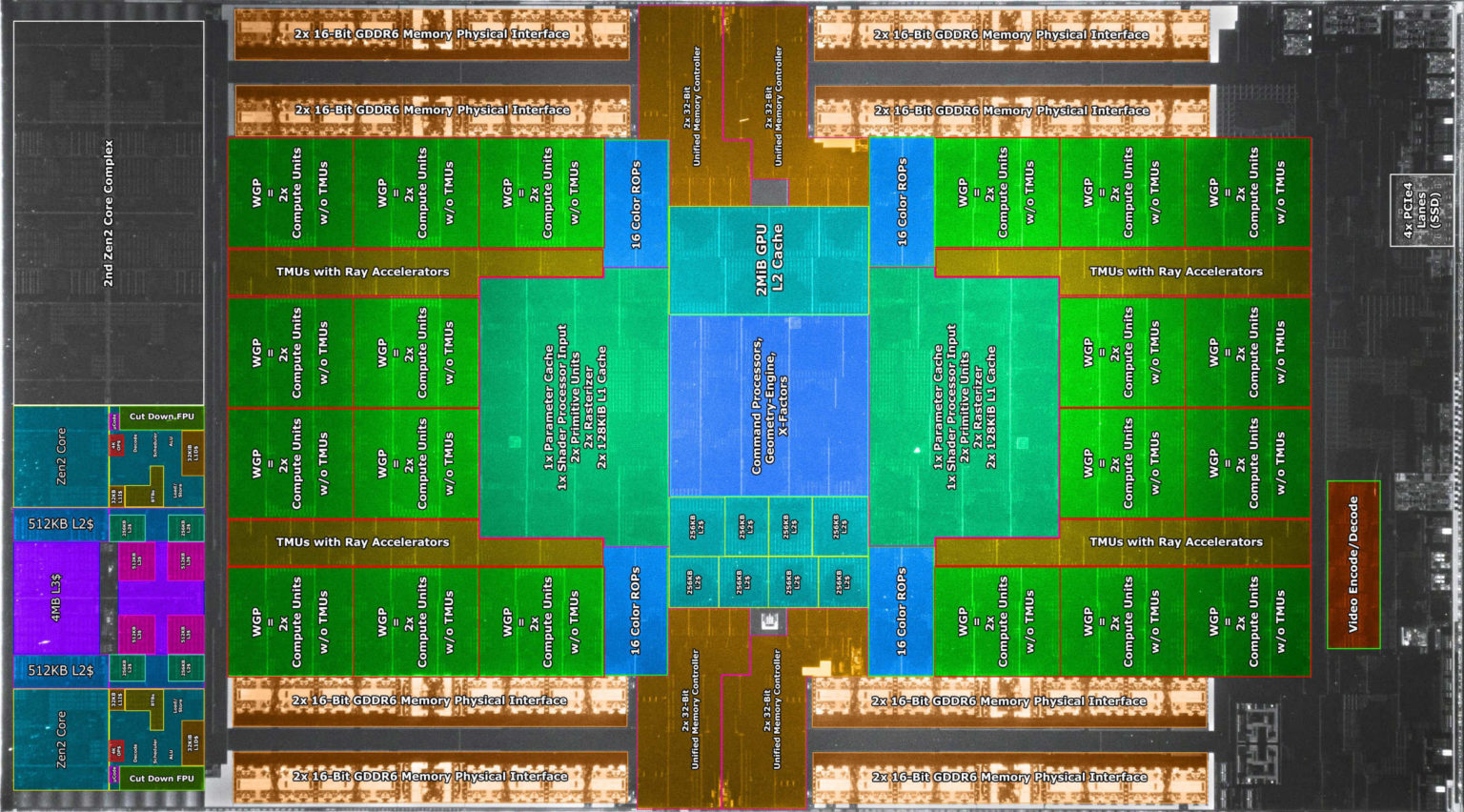
PS5 SOC, with the Zen2 cores on the left:
PlayStation-5-die-close-marks-1536x852.jpg

source: https://videocardz.com/newz/sony-playstation-5-soc-die-pictured-up-close

An 8-core Zen2 die is called a CCD and is divided into two groups of 4 cores. Each group of 4 cores is called a CCX. On desktop, each CCX has 16MB of L3 cache. Console variants have 8MB per CCX. On Zen2, if a CCX wants to access the L3 cache on the other CCX, it still has to go out to the central IO die, which is very inefficient (Anandtech). Hence why Zen3 merged the L3 caches. Indeed, a future iteration of Zen3 is reported to triple the size of the L3 cache: an additional 64MB of cache per core cluster (Reddit).

PS5 I believe is based on the 4700G. The Zen2 desktop was the 3000 series, Zen2 mobile was the 4000 series. In contrast, the 5000 series simplifies the naming by encompassing both Zen3 desktop and mobile CPUs.

As to why both consoles don't have the large L3 caches of desktop CPU: it eats up huge amounts of die space. They're competing for transistors with the GPU so console designers have to balance the demands of both.
 
Last edited:
So they only load , parts of the new level , in rifts .. as expected, so it doesn’t load 16 gigs . As I talked about in the past here, and stream the other parts in when needed.

Some of that memory is reserved for the system so developers can never use the whole 16GBs. What they did say is that depending on the type of rift/transition influences the amount that's loaded. So if it's one of the ones with a short rift animation they have the ability to dump everything loaded in memory in the previous area and load everything that's needed in the next one. The only thing thats maintained in memory are the constants like the character you control for example.

In other worlds if they use 10GBs for the last area they can dump that for 10GBs of data for the next one. And even then they can just loaded part of the next area instead of the whole thing which affects the size of the data.

Pretty interesting how everything is put together.
 
Top Bottom