-
Hey, guest user. Hope you're enjoying NeoGAF! Have you considered registering for an account? Come join us and add your take to the daily discourse.
You are using an out of date browser. It may not display this or other websites correctly.
You should upgrade or use an alternative browser.
You should upgrade or use an alternative browser.
Ken Kutaragi is the Greatest 'emperor' Of All Time and remains SIE's only true visionary
- Thread starter GAF machine
- Start date
- Opinion
Negotiator
Member
I always had the suspicion that Cell was a proto-GPGPU and it seems there is some hard evidence about it:Sounds awfully similar to nVidia's DLSS-style solution for AI video upscaling, don't you think?

Pixel Perfect: RTX Video Super Resolution Now Available for GeForce RTX 40 and 30 Series GPUs
Learn how RTX Video Super Resolution uses AI to improve streaming video in latest Game Ready Driver for GeForce RTX 40 and 30 Series GPUs.blogs.nvidia.com
Of course that won't get you very far if the plebs don't understand your vision... let alone when your hardware has a very immature software stack that cannot demonstrate the hardware's benefits.
I'd argue Crazy Ken was way too far ahead of his time for his own good. His vision was extremely similar to Leather Jacket Man™, but nVidia has had far better execution so far (that's why their market cap is worth over 3 trillion $, while Sony is barely worth 100 billion $).
He clearly wanted Sony to become something bigger by using the PS3 as a trojan horse... who knows, maybe in a parallel universe Sony is worth 3 trillion $ and CUDA never took off.
Kutaragi talks PS3 backward compatibility, disses 360 (again) - News at GameSpot
for News at GameSpot. GameSpot provides in-depth news about and hundreds of other games, including game announcements, developer interviews, screenshots, sales figures, hands-on impressions, video interviews, and movies.
web.archive.org
IPW: First of all, why did you select Nvidia as your GPU vendor?
KK: Up until now, we've worked with Toshiba [for] our computer entertainment graphics. But this time, we've teamed with Nvidia, since we're making an actual computer. Nvidia has been thoroughly pursuing PC graphics, and with their programmable shader, they're even trying to do what Intel's processors have been doing. Nvidia keeps pursuing processor capabilities and functions because [Nvidia chief scientist] David Kirk and other developers come from all areas of the computer industry. They sometimes overdo things, but their corporate culture is very similar to ours. Sony and Nvidia have agreed that our goal will be to pursue [development of] a programmable processor as far as we can. I get a lot of opportunity to talk to Nvidia CEO Jen-Hsun [Huang] and David, and we talk about making the ideal GPU. When we say "ideal," we mean a processor that goes beyond any currently existing processor. Nvidia keeps on going into that direction, and in that sense, they share our vision. We share the same road map as well, as they are actually influenced by our [hardware] architecture. We know each other's spirits and we want to do the same thing, so that's why [Sony] teamed with Nvidia. The other reason is that consumers are starting to use fixed-pixel displays, such as LCD screens. When fixed-pixel devices become the default, it will be the age when TVs and PCs will merge, so we want to support everything perfectly. Aside from backward compatibility to, we also want to support anything from legacy graphics to the latest shader. We want to do resolutions higher than WSXGA (1680x1050 pixels). In those kinds of cases, it's better to bring everything from Nvidia rather than for us to create [a build] from scratch.
Thanks for the link, you're a living Ken encyclopedia.
")
Also this:
NVIDIA's Sony relationship will go beyond PS3
David Kirk, chief scientist at NVIDIA and leader of the teams behind the GeForce 7800 and PS3 graphics chips, has revea…
D DonkeyPunchJr
What were you saying...?
I think it's fair to say that CUDA/GPGPU would have never been the same without Sony's contribution with Cell.
Same for ATi/AMD (8 ACEs, Asynchronous Compute etc.)
Cell's legacy still lives on. Just like dinosaurs disappeared, but modern day birds still carry dinosaur DNA.
reinking
Gold Member
That will not stop it from happening. Look at all of the awards he has received.Phil Spencer has literally contributed nothing creative or interesting to the video games industry.
Rocco Schiavone
Member

Hugare
Member
Crazy Ken is a legend
I miss visionaries like him in the industry today. Dude knew the risks and said "fuck it", spent dont even know how much on R&D to make a chip that was like nothing else at the time. It takes some huge balls to do something like this.
PS3's architecture was a bitch to develop to, but at the right hands, it generated incredible stuff. Uncharted 2/3, MGS 4, God of War 3 ... these games were events. You wouldnt see games like those on the competition.
I was always eager to see what those unique architectures could do. People theorized about the limits of the chip. Nowadays everything is so obvious and boring. Consoles are already outdated at launch, and their hardware's limits are known since announcement.
Gaming in general became so predictable, samey and safe. Ken is an icon of better times.
Last edited:
I'm pretty sure Sony headsets already do this ( I know my XM4 asked for a picture of my ears for 360 Reality Audio) :We also know (according to Cerny) that the PS5 is fully capable to use custom/personalized HRTF profiles by analyzing a photo of your ears (this would probably require a cloud AI backend that costs tons of money):
But Cerny said "years down the line" we might be able to use this in games with a profile on the console.
Last edited:
Negotiator
Member
Another notable mention:

 en.wikipedia.org
She's the Amy Hennig of hardware in my eyes.
You won't see any feminists praising her... there were no diversity hires back then, just pure brains, 100% meritocracy.
No wonder AMD was saved under her leadership. One of the few female CEOs that deserves her role.
AMD HSA/hUMA (Fusion/APUs) is a byproduct of her expertise in Cell development.
So even with a Sony headset it's not usable in games?
Either way, with 50 million PS5s sold we have 100 million ears to analyze (potentially even more if you have more accounts/users on a single console), so this is gonna require a beefy AI backend.
Unless Sony decides to form a p2p AI network where the PS5 GPUs will actually do the AI training (not very likely to happen, but this was supposed to be Ken's vision with Cell).
Lisa Su - Wikipedia
Through her division, Su represented IBM in a collaboration to create next-generation chips with Sony and Toshiba. Ken Kutaragi charged the collaboration with "improving the performance of game machine processors by a factor of 1,000", and Su's team eventually came up with the idea for a nine-processor chip, which later became the Cell microprocessor used to power devices such as the Sony PlayStation 3. She continued as vice president of the semiconductor research and development center at IBM,[6] holding the role until May 2007.
She's the Amy Hennig of hardware in my eyes.
You won't see any feminists praising her... there were no diversity hires back then, just pure brains, 100% meritocracy.
No wonder AMD was saved under her leadership. One of the few female CEOs that deserves her role.
AMD HSA/hUMA (Fusion/APUs) is a byproduct of her expertise in Cell development.
Interesting, but Cerny insinuated we would have this with any regular stereo headset, since Tempest Audio doesn't require a proprietary Sony headset.I'm pretty sure Sony headsets already do this ( I know my MX4 asked for a picture of my ears for 360 Audio) :
But Cerny said "years down the line" we might be able to use this in games.
So even with a Sony headset it's not usable in games?
Either way, with 50 million PS5s sold we have 100 million ears to analyze (potentially even more if you have more accounts/users on a single console), so this is gonna require a beefy AI backend.
Unless Sony decides to form a p2p AI network where the PS5 GPUs will actually do the AI training (not very likely to happen, but this was supposed to be Ken's vision with Cell).
Last edited:
Fahdis
Member

MF just blinked and disguised it as a sexual wink.
cinnamonandgravy
Member
yeah but sony said it, as ridiculous as it is. same silly people who said PS3 would have two hdmi-outs for dual 1080p output and the controller would be a boomerang.Only silly people thought CELL would be in toasters. It wasn't made to suit kitchen appliances. It was made to suit networked appliances purpose-built to process and display media.
and three ethernet ports. one was probably for toasters.
Last edited:
Negotiator
Member
This was silly from the get-go.yeah but sony said it, as ridiculous as it is. same silly people who said PS3 would have two hdmi-outs for dual 1080p output and the controller would be a boomerang.
and three ethernet ports. one was probably for toasters.
Back in 2002 I was able to buy a 5-port Ethernet switch for $35. Now it's 3-4 times cheaper, with Gigabit and up to 8 ports.
Also, Ken had made some outrageous claims about 120 fps:
PS3 could run at 120 fps
Sony Computer Entertainment boss Ken Kutaragi has claimed that the PlayStation 3 will run games at an unprecedented (an…
I mean, I'm glad we got Uncharted 1-2-3 & TLOU1 at 720p 30 fps, there was no need to make outrageous claims. Even the HDMI chipset didn't support 120 Hz, AFAIK.
The boomerang controller (with no vibration!) was moronic. They had some patent issues and then DualShock 3 came out.
nial
Gold Member
I appreciate the well-put response, but a month later I just can't bring myself to care enough.Kutaragi is one of SCEI's founders, so the company’s culture was partly of his making. Ozawa was mainly a titular head. Shuji Utsumi (VP of product acquisition at the time) divulged that once Kutaragi got approval from Norio Ohga to create PS1 "Ken’s career went from almost zero [to essentially running Sony Computer Entertainment]."
Shigeo Murayama (SCEI Chairman, previous SMEJ CEO) disclosed that his role was simply to setup a "comfortable working environment" for him, and maintains that Kutaragi was "the engine behind it all".
Kutaragi gets credit for more than PS1's hardware. Here he is in his own words...
"Yes, I was the starting engineer, and many times I have been called the "father of PlayStation". But I also work in the software department, so I have also been involved with the hiring of people for Sony's software development — and this has been ongoing since the PlayStation design was finished".
"As well as being an engineer, I have been involved in the business side of things for many years. I helped start the company, and I have always been involved in business decisions".
I'd be remiss if I didn't point out that one of the business decisions he was involved in was setting PS1's price at $299. Kutaragi was the mind and muscle behind SCEI's operations from the start.
Nope. Kutaragi handled PS2’s planning from start to finish...
'That freedom of initiative has continued with the development of PS2. Sony president Nobuyuki Idei didn't see a solid plan for the machine until just a few weeks before its development was announced in March 1999. "Nobody in top management knew what we were up to," says Kutaragi. In fact, he had started working on PS2 as soon as the first-generation PlayStations were being unpacked from their boxes. He called together a few dozen engineers from all over the world, including Toshiba's team, to a secret meeting in the city of Ito in 1996. There, Kutaragi divulged his dream of turning PlayStation into a platform for connecting an increasingly wired world.' -- Time
I know you think he did a lot more harm than good, but you can at least be factual.
I don't think much of this post refutes what I said, and it's just you overfocusing too much on very specific compliments. Stuff like his involvement in the software departments doesn't really read like him making the top decisions, but rather acting as a consultor of some kind; which makes sense, because he's almost never credited in any 1994-1999 SCEI game.
Nah, I do not think that, I believe he used to be a very integral part of the business, especially in such a hardware-focused company like SIEI, but he didn't do a very good job once he got to the top in April 1999.I know you think he did a lot more harm than good, but you can at least be factual.
Last edited:
GAF machine
Member
I always had the suspicion that Cell was a proto-GPGPU and it seems there is some hard evidence about it:
Kutaragi talks PS3 backward compatibility, disses 360 (again) - News at GameSpot
for News at GameSpot. GameSpot provides in-depth news about and hundreds of other games, including game announcements, developer interviews, screenshots, sales figures, hands-on impressions, video interviews, and movies.web.archive.org
Here’s a little more evidence to confirm your suspicion…
Another notable mention:
Lisa Su - Wikipedia
She's the Amy Hennig of hardware in my eyes.
You won't see any feminists praising her... there were no diversity hires back then, just pure brains, 100% meritocracy.
No wonder AMD was saved under her leadership. One of the few female CEOs that deserves her role.
AMD HSA/hUMA (Fusion/APUs) is a byproduct of her expertise in Cell development.
Yeah, Su’s made quite a name for herself. She's certainly an industry titan. Props to her for helping stand up the STI Design Center where CELL was R&Ded, but it wasn't her team that designed CELL.
James A. Kahle (Jim Kahle) was head honcho of the CELL project. That's why Kutaragi selected him to deliver a pre-recorded message about CELL for PS3's reveal.
As for Fusion, it long predates Su and AMD already knew it was similar to CELL before she arrived...
Also, Ken had made some outrageous claims about 120 fps:
PS3 could run at 120 fps
Sony Computer Entertainment boss Ken Kutaragi has claimed that the PlayStation 3 will run games at an unprecedented (an…www.eurogamer.net
He didn't make the claim. Ellie Gibson/Eurogamer claimed that he made the claim. In the original article about the event that Eurogamer falsely reported on, there's a section titled: 120フレーム/秒の映像を送出'. If you translate (I use DeepL) the title and section you’ll see that he was talking about PS3 transmitting video at 120 fps, and using a high-speed camera with PS3 to analyze video frames at 120 fps for game inputs. He doesn't claim that PS3 will run games at 120 fps.
Richard Marks (PS Eye's creator) explained that the PS Eye camera has a 120 fps mode to do just that.
Eurogamer published an article years later about Super Stardust 3D running at 120 fps as if to say a promise was kept, but Kutaragi never said PS3 could or would run games at 120 fps in the first place.
I mean, I'm glad we got Uncharted 1-2-3 & TLOU1 at 720p 30 fps, there was no need to make outrageous claims. Even the HDMI chipset didn't support 120 Hz, AFAIK.
Eurogamer: What you're doing here is something I can really appreciate... taking something that's there in the home and being pushed beyond its original design specifications. Although having said that, the original PS3 specs talked about dual HDMI ports and 120Hz outputs. Ken Kutaragi really was thinking ahead of his time there.
Ian Bickerstaff: When I joined Evolution Studios, that was one of the reasons I joined. It's got two outputs! Connect that to two projectors and you've got 3D! It's ironic because the format that's now in PS3 is actually much more elegant and simple than that. Only one HDMI but it's producing that quality. It was a happy ending but it was a little annoying when I discovered that they'd removed that second HDMI port.
Last edited:
GAF machine
Member
yeah but sony said it, as ridiculous as it is.
That "CeLl BrOaDbAnD eNgInE wIlL bE iN a ToAsTeR" nonsense came from sillies (like Gunbuster) on the internet.
Where’s the toaster?...
Last edited:
Jinzo Prime
Member
A quote from J Allard (former Xbox vice president) back in the day:
"What gets me out of bed and into the office every day is the thought of Ken Kutaragi's resignation letter, framed, hanging next to my desk."
We need this level of hate back in the console space, this is what lead to some ot the best games of all time. Now everybody's singing kumbaya and competition is dead.
GAF machine
Member
I respect the guy (I would even call myself a fan) a lot but he is obviously not perfect.
No one’s perfect. Kudos to him for being imperfect when he stuffed PS3 with technologies that support PS4, PS4 Pro, PS5 and PS5 Pro at a fundamental level.
GAF machine
Member
I appreciate the well-put response, but a month later I just can't bring myself to care enough.
I don't think much of this post refutes what I said, and it's just you overfocusing too much on very specific compliments. Stuff like his involvement in the software departments doesn't really read like him making the top decisions, but rather acting as a consultor of some kind; which makes sense, because he's almost never credited in any 1994-1999 SCEI game.
Despite your apathy, I'll leave you with this:
They aren't compliments. They are accounts of what he did during SCEI's formative years.
If he was in a position to hire people for software development, then he was in a position to make decisions about software that he wanted to define his hardware.
If he had the authority to shift factory lines from pressing music CDs to pressing Tekken and other games, then he had the authority to make decisions about when games would be on his hardware.
If Steve Race and Teruhisa Tokunaka deferred to him about PS1's business model and $299 price point, then Kutaragi was essentially acting as CEO, not some consultant.
I seriously doubt he cares about rarely being credited in games from '94 - '99. He has the ultimate credit of being the "father of PlayStation" for all-time, and of being the person responsible for making the brand a household name.
Funny, while Tokunaka and Maruyama were trying to shine in game credits as executive producers, Kutaragi was trying to shine the light on and give credit to the creators who made the games.
Nah, I do not think that, I believe he used to be a very integral part of the business, especially in such a hardware-focused company like SIEI, but he didn't do a very good job once he got to the top in April 1999.
There was never a time when he wasn't at the top.
Last edited:
Negotiator
Member
It'll be classified as "toxic masculinity" in a heartbeat and you know it.We need this level of hate back in the console space, this is what lead to some ot the best games of all time. Now everybody's singing kumbaya and competition is dead.
The whole industry has been effeminized...
Fuck it, I want David Jaffe and CliffyB back!
I don't want the modern woke Jaffe, I want the good ol' Jaffe of the PS3 era:
Jaffe Defends PSP2 like 'Fresh Pussy" Comment
Look everybody, let's all just chillax, yeah? - David Scott Jaffe of God of War and Twisted Metal (the reboot, re-hash, whatever) has come out in defence of David Scott Jaffe's statement that Sony's new portable...click for more
spong.com
Thanks for the detailed response once again!
You're right about 3DTV/120 Hz (the HDMI controller was programmable with a newer firmware update) and I know 3D still kinda lives on PSVR1/2, but I miss 3DTVs too.
PSVR is too "solitary" unlike 3DTVs where multiple people can enjoy them. Hell, with 4K and passive glasses we could have had a nice 1080p3D experience with minimal cost.
It's a shame 3DTVs were abandoned.
AeonGaidenRaiden
Member
Ken was a snake oil salesman. He just made up BS comments about what the console could do when it could never reach those highs. PS3 managed to turn it around in the end barely but imagine if there was less BS and they continued their upward trajectory from the PS2. They literally had a fall off same as Xbox360 to XboxOne. PS3 could of been the highest selling console till the end of time. He killed any momentum they had necause he was making up shit without knowing how development works. In general CEOs are businessmen pretending to be gamers. Remember Reggie and getting bodyied is Smash Bros by a fan when saying how he plays the game every day? He looked like he picked up the gamecube controler for the first time ever.
Last edited:
Tiago Rodrigues
Member
A leader doesn't send a company to die like he almost single handily did for Sony, lmao.Great times when Sony had true leaders. Unlike the actual pussies like Herman
Damn nostalgia really is a thing
Negotiator
Member
Xbone never recovered though, nor it has any memorable classics.Ken was a snake oil salesman. He just made up BS comments about what the console could do when it could never reach those highs. PS3 managed to turn it around in the end barely but imagine if there was less BS and they continued their upward trajectory from the PS2. They literally had a fall off same as Xbox360 to XboxOne.
Yes, in the end PS3 sold more than XBOX 360, despite the latter selling quite a few replacement consoles due to RROD (YLOD was less prevalent).
The only failed console by Sony was PS Vita (close to Wii U numbers).
If PS3 was as successful as the PS2, we would have seen more die shrinks (Cell @ 32nm never happened for unknown reasons, despite RSX getting down to 28nm with 2 GDDR5 chips @ 64-bit bus) and the next-gen Cell 2 successor (2 PPEs, 32 SPUs @ 1 TFlop).
Any idea what prevented Cell from having more die shrinks? What was the technical hurdle? I vaguely remember something about the EIB bus, but I'm not 100% sure.
PS3 Cell chip being shrank from 45nm to 22nm, when will we see this?
So, a lot of evidence (in a quote box below for the sake of tidiness) points to development of the PS3's Cell chip which has shrunk it from a 45nm size to 22nm. "Elizabeth Gerhard's Projects PlayStation 3 Team Members: Elizabeth Gerhard - Owned the array design for a 1.6GHz TLB array in...

Chen Chu - Apple | LinkedIn
Results-driven Electrical Engineer with a strong background in mixed-signal and digital… · Experience: Apple · Education: University of California, Los Angeles · Location: San Jose · 255 connections on LinkedIn. View Chen Chu’s profile on LinkedIn, a professional community of 1 billion members.
 www.linkedin.com
• PS3 Cell processor – migration to 22nm
- Responsible for top-level large-block synthesis of the entire SPU (Synergistic Processing Unit).
- Achieved route-ability and timing closure through sophisticated synthesis techniques involving detailed floor-planning, custom pre-wires and register placement, custom routing algorithms, and placement boundaries.
• XBOX PowerPC chip – migration to 32nm
- Helped to develop the flow for schematic and layout migration of key custom arithmetic and control circuits.
- Led efforts to execute and trouble-shoot the extensive sign-off flow for both custom and synthesized circuits (enabling myself and the team to pass all checks ahead of schedule).
- Led migration of the analog/mixed-signal Random Number Generator unit. Played a key role in fixing feedback within the RNG CHAOS block.
Looks like XBOX 360 made it all the way down to 32nm (a single die for Xenon CPU + Xenos GPU + eDRAM):

Next Xbox's 32nm CPU enters production - Report
Tech news site indicates IBM, Global Foundries now manufacturing "Oban" chip for dev kit delivery by April.
 www.gamespot.com
Oban - XenonLibrary
 xenonlibrary.com
Imagine a dirt cheap single-die PS3 at $99 or even less... would it ever be possible? (considering the fact PS3 had 2 separate memory buses/technologies: XDR + GDDR3, unlike XBOX360 having a unified GDDR3 memory)
Last edited:
Negotiator
Member
Also just found this:

AMD CEO Lisa Su reminisces about designing the PS3's infamous Cell processor during her time at IBM
Even before she worked at AMD, Lisa Su was making big moves and proving to be one of PlayStation's greatest allies
Did they collab with Jim Kahle?

cartman414
Member
Crazy Ken is a legend
I miss visionaries like him in the industry today. Dude knew the risks and said "fuck it", spent dont even know how much on R&D to make a chip that was like nothing else at the time. It takes some huge balls to do something like this.
PS3's architecture was a bitch to develop to, but at the right hands, it generated incredible stuff. Uncharted 2/3, MGS 4, God of War 3 ... these games were events. You wouldnt see games like those on the competition.
I was always eager to see what those unique architectures could do. People theorized about the limits of the chip. Nowadays everything is so obvious and boring. Consoles are already outdated at launch, and their hardware's limits are known since announcement.
Gaming in general became so predictable, samey and safe. Ken is an icon of better times.
High development skill floors with high performance ceilings (yeah, borrowing metagame lingo, suck it) were no longer worth the trouble, if not no longer a thing.
EDMIX
Writes a lot, says very little
In context, that was actually true at launch. PS3 cost of manufactor was around 800$ and was sold for 600$. The Bluray player on PS3 was on par with a 1000$ standalone bluray players, and even had the advantage of possible improvements by firmware updates.
But all this just made Playstation divison going to the red for like 3 or 4 years untill they started cutting feautures from the OG console and the bluray tech got cheaper.
Truth
I feel Bluray was 100% needed and calculated. Games get bigger each gen, not smaller and they needed a new format and looking at how cheap bluray is now and that is its in XB, PS etc, it was ahead of its time and he was forward thinking to take the hit then, of a format needed in the future.
But I felt that all the way back in 2006.
I got that it was expensive, but i saw it as PS2 having DVD as being expensive, sure they could have used CD again to be cheap, you some of you sure thats the lazy ass leap you want to save some bucks? Only to spend the whole gen crying about how not much advanced or something?
So someone needed to take that hit and it was a calculated one that paid off for em.
So taking risk can be expensive and I'd rather someone bite the bullet to push those boundaries then looking to be cheap
Gojiira
Member
Well just look at the the sheer amount of Phil Spencer threads…One thread about Ken is hardly shillingAnd people think only Microsoft pays for shills here?

Hugare
Member
The results speak for themselves, imoHigh development skill floors with high performance ceilings (yeah, borrowing metagame lingo, suck it) were no longer worth the trouble, if not no longer a thing.
GOW 3 and Uncharted 3 looked better than some games from the PS4 generation.
That may be the case due to how good these devs were at the time, and not because of the hardware, but imo the hardware was hugely important. We wont be 100% sure tho.
Negotiator
Member
God of War Ascension looks even better than GoW 3:The results speak for themselves, imo
GOW 3 and Uncharted 3 looked better than some games from the PS4 generation.
That may be the case due to how good these devs were at the time, and not because of the hardware, but imo the hardware was hugely important. We wont be 100% sure tho.
I mean, take a close look at Kratos' textures.
I can't believe they achieved such a texture quality with only 256MB of VRAM...
It's truly a shame this game is platform-locked on PS3 and there's no PS4/5 remaster.
Do you guys think that the PS6 could perhaps have a beefy Zen 4/5 8-core CPU with full AVX-512 support @ 3.5 GHz?
RPCS3 runs a lot smoother with AVX-512:
Sony will eventually need to retire those old PS3 motherboards on PS Now/PS+ Premium:

Sony creates custom PS3 hardware for PlayStation Now
Sony has developed brand new PS3 hardware to power its PlayStation Now streaming service, revealed earlier this month a…
Do they still manufacture Cell/RSX chips in 2024? I strongly doubt it, but maybe I'm wrong.
Last edited:
GAF machine
Member
Did they collab with Jim Kahle?
STI leadership (especially Kutaragi) collabed with Kahle to hash out CELL's particulars. AMD wasn't involved.
Thanks for posting the Su interview/CELL commentary in the thread. There’s a really old interview (originally posted on B3D, posted on GAF a couple days later) with Su and Kahle that you may not have seen. It discusses the CELL project from their perspective. I'll repost it below, make it more orderly and bold some parts I found interesting...
A Cell of a chip
Key players weigh in
Lisa Su, vice president of technology development and alliances, STG, and Jim Kahle, IBM Fellow and lead architect for Cell, STG, have been involved with the Cell project from day one. Here are their thoughts on some significant aspects of this announcement.
Project history
Lisa Su: We announced the Austin design center with Sony and Toshiba in March of 2001, and before that we spent about a year defining the architecture. It was unique in that we had the ability to start with a clean sheet of paper, under the direction of both Ken Kutaragi of Sony and John Kelly of IBM. ISSCC marks the first time we are talking about the technical details of the project.
Jim Kahle: With the clean sheet, we stepped back and looked at a number of aspects of the Cell, such as chip design, system design and power management. The partnership allowed us to think outside of the box. And the consumer electronics link gave us a new level of human interchange, and a new way of designing computers.
Key details
JK: The magnitude of the multi-core design is very important. Each cell chip has nine processors on board, and with the central Power core having two threads, it's more like a 10-way processor model. We optimized the whole system architecture around multi-core, taking the chip to the next level of performance.
LS: Cell represents a confluence of lots of technologies. For instance, virtualization allows multiple operating systems to run at the same time, including open operating systems such as Linux. In designing Cell, we employed techniques that were developed over many years for use in our high-end Power servers, but with the advances of semiconductor technology, we are able to bring these techniques into consumer devices. This will enable a whole new set of applications that have yet to be developed.
Prospective uses
JK: Cell's synergistic process elements, or SPEs, are able to handle large amounts of graphics, improving media processing capability. In addition, the chip will be able to manage compute-intensive type applications.
LS: Cell will enable a wide range of applications, such as next-generation game machines, home servers and digital media servers. A smaller version of Cell could conceivably be used for HDTV, and a larger version for content-creation workstations for the entertainment industry or even scientific computing applications.
Chip speed
JK: We've seen speeds of Cell greater than 4 GHz in the lab, and speeds of isolated SPE as high as 5.6 GHz. We approached the design with the idea of attaining high-performance frequency.
LS: You might want to think of Cell as the world's "most powerful" chip. And although frequency is important, even more important is the parallelism and being able to run on nine cores allows the ability to do a large number of operations simultaneously.
Power Architecture
LS: It was important for Sony and IBM to start with a mature architecture for the general purpose microprocessor core so that we could build on a stable programming base. And since IBM's strategy is to have an open Power Architecture, this is an excellent example of how the Power Architecture can be leveraged into new markets such as the gaming and entertainment industry.
JK: Power Architecture is a great base for conventional processing and we extended its capabilities for extreme media processing and real-time behavior for human interactions. It adds a whole new dimension on how to program.
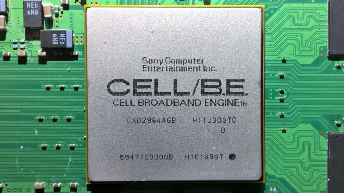
Production
LS: Cell will be a 90 nanometer SOI chip with more than 230 million transistors, and will be produced both in the 300mm fab in East Fishkill and Sony's 300mm fab in Nagasaki. We'll start production in 2005.
JK: As far as OEM is concerned, we'll approach the industry through IBM Engineering & Technology Services for third-party services and applications, and we have already received significant interest.
Growth opportunities
JK: Cell technology will allow IBM to go into new and emerging areas, and show leadership in the gaming area. This is a tremendous opportunity for all three companies.
LS: Cell uses the strength of all three partners and it starts with IBM's leadership silicon-on-insulator technology and microprocessor design expertise, combined with Sony's market and system insight and Toshiba's semiconductor experience and to apply this technology in new markets, such as digital media, entertainment and consumer electronics. It is a great example of the "sum is greater than the individual parts." Sony is one of our deepest technology partners and we've spent a combined $400 million in joint microprocessor development with Sony and Toshiba, Sony and Toshiba are partners in our SOI process development alliance, and Sony has invested $325 million in the fab in East Fishkill.
Confluence of technology
LS: We often refer to the confluence of technology in Cell. That includes features like high frequency, parallel multi-thread, efficient architecture and state-of-the-art virtualization. When you think about it, it's pretty amazing to have this type of chip and this type of processing power going into a game system.
JK: And we've also added autonomic power management, real-time resource management for human interaction and smart memory flow controllers.
source
Any idea what prevented Cell from having more die shrinks?
Sony will eventually need to retire those old PS3 motherboards on PS Now/PS+ Premium:
Do they still manufacture Cell/RSX chips in 2024? I strongly doubt it, but maybe I'm wrong.
CELL is probably already at 14nm, with a possible path to 7nm. Here comes another detailed spiel...
2012 - 2014 - IBM supplies SIE with 22nm SOI CELLs. SIE builds PS3 server boards with them to prepare for PS Now's launch in 2014.
2014 - IBM sells its semiconductor business to GlobalFoundries. GF becomes IBM's supplier of 22nm SOI POWER8 chips with the goal of 14nm and 10nm chips down the road.
2017 - GF and IBM jointly develop a 14nm FinFET/SOI (14HP) process. IBM uses it for POWER9 and z14 CPUs
2017 - GF skips 10nm, announces 7nm (7LP) FinFET which is said to have a high level of overlap with the 14HP process
2018 - GF halts further 7nm development indefinitely to focus on 14nm/12nm essential and specialty chips
2020 - Kenichi Nakano (General Manager of Sony Semiconductor Solutions managing GNSS products, unique SoC products, and LTE related products) chooses GF's 22nm FDX process for Sony's GNSS chips. Selecting GF (now owner of IBM's SOI process) gives SIE the ability to extend Kutaragi's CELL roadmap to 14nm (14HP) FinFET SOI and 7nm (7LP) FinFET bulk, which is just waiting for an investment in what's left of its development to create a 7nm FinFET SOI (7HP) process.
At this stage in its life, CELL is a specialty chip (only used for the PS Now platform) that's always been a unique SoC. In '13, Masayasu Ito said that SIE could “freely manufacture CELL if the decision is made that it is needed”, but support components "will become difficult to obtain since 7 years is already considered to be long in the IT industry". Surely, some of those components must be getting nigh on impossible to obtain now. I think component scarcity, PS Now's ageing fleet of 22nm PS3 servers and a desire to have more CELLs per wafer drove SIE to quietly redesign and migrate CELL (and likely the RSX) to GF/IBM’s 14HP process at some point in ’21. SIE probably has stockpiles of 14nm PS3 replacement servers ready to deploy.
Imagine a dirt cheap single-die PS3 at $99 or even less... would it ever be possible? (considering the fact PS3 had 2 separate memory buses/technologies: XDR + GDDR3, unlike XBOX360 having a unified GDDR3 memory)
There was a time when I thought SIE would make a $99 - $149 PS3 attachment, but no longer. Not because of any real or imagined technical challenges. I've just come to the conclusion that SIE has moved on from PS3 hardware, save for PS Now.
The only PS3s SIE cares to make are the ones fit for PS Now server boards.
God of War Ascension looks even better than GoW 3:
I mean, take a close look at Kratos' textures.
I can't believe they achieved such a texture quality with only 256MB of VRAM...
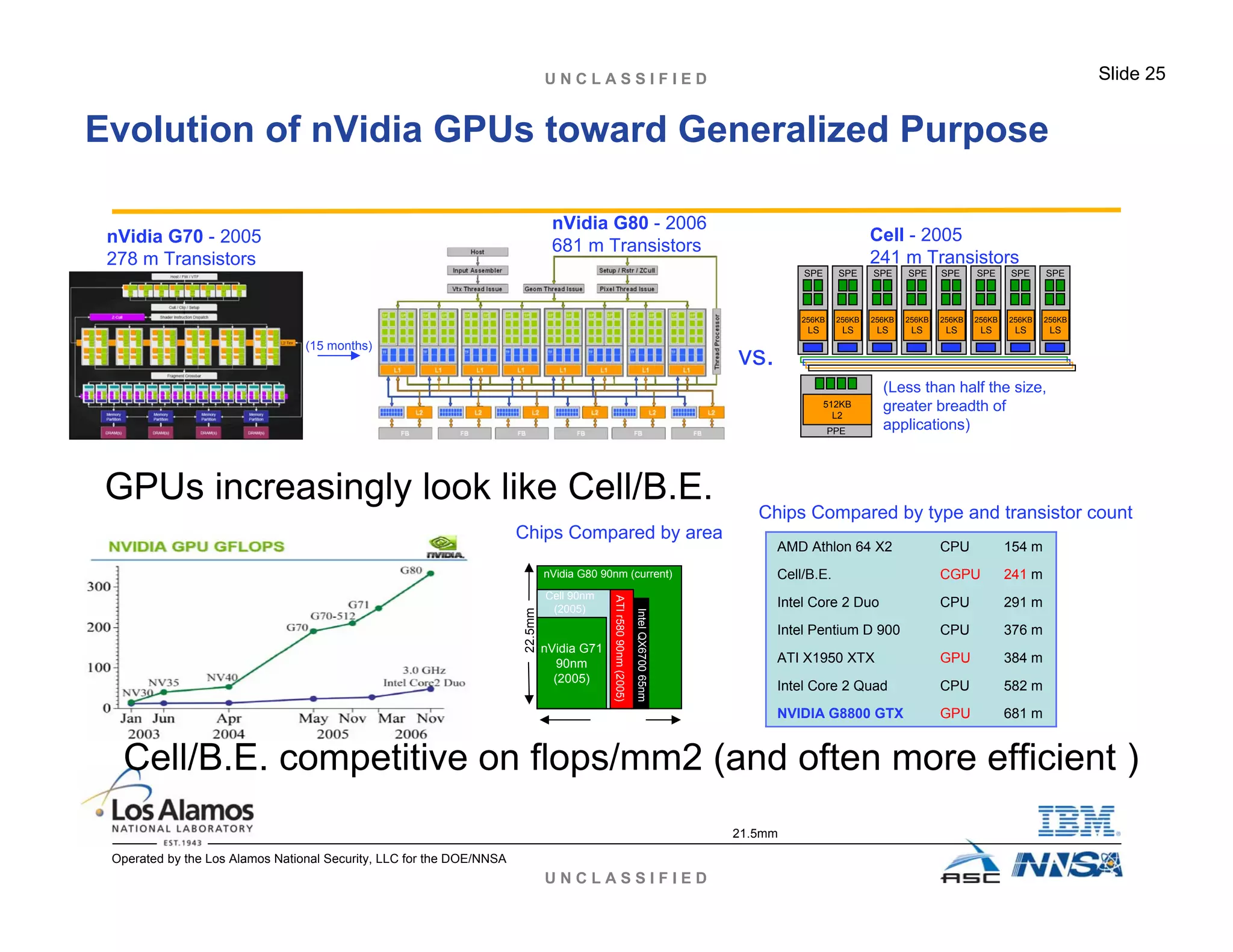
More like 512MB of DRAM + VRAM. Contrary to popular belief, PS3’s memory is unified. It’s just physically split between XDR and GDDR3. A whitepaper by two SCEA researchers explained: "The system's unified memory architecture allows the Cell/B.E. and GPU to exchange data through shared textures"... "This system combines the Cell/B.E. with a state of the art GPU in a unified memory architecture. In this architecture both devices share access to system memory and to graphics memory. As a result they can share data and processing tasks". The researchers went on to describe PS3's architecture as a "hybrid real time rendering system".
The best devs exploited PS3's hybrid real-time rendering system to their utmost. Santa Monica Studio was certainly one of the best…
Also, CELL’s heterogeneity and simultaneous access to XDR and GDDR3 memories made PS3’s hybrid real-time rendering system a HSA with hUMA long before AMD made the terms 'HSA' and 'hUMA' marketable. PS3 was a marvel of engineering.
Do you guys think that the PS6 could perhaps have a beefy Zen 4/5 8-core CPU with full AVX-512 support @ 3.5 GHz?
RPCS3 runs a lot smoother with AVX-512:
I wouldn't rule it out, but geez. Wouldn’t that be a ton of heat to dissipate and exhaust from a console form-factor? That PS6 would probably need liquid metal and dual fans whistling/blowing like a KLM at takeoff power to keep cool.
I doubt SIE can do much better than the inconsistent RPCS3, despite everything they know about CELL. Jacob Stine (of PCSX2 fame, former SIE, now Implicit Creations) filed for an emulator that uses a JIT compiler to remap the functions of a target (e.g. a SPU core) to a host CPU (e.g., a Zen 2 core).
Entry [0043] reads: The Target System may include processor units which are incompatible with the Host CPU 400, for Example Vector Processing units or Synergistic Processing Units which will have their functions remapped for the architecture of the Host CPU core 400 by the JIT compiler during emulation of the target system.
SIE’s been sitting on this for 7 years (there's that number again), yet we haven't heard peep nor squeal from them about PS3 backwards compatibility. I think SIE is mum because Zen 2 can’t emulate CELL to a satisfactory degree, whatever SIE deems satisfactory.
That’s why I gave up hope of a PS3 emulator for PS5 a long time ago. Zen 4/5 doesn't change that for me.
I think a redesigned, integrated 14 or 7nm CELL that doubles as an AI accelerator or other special use processor is the surest way to PS3 backwards compatibility on PS5 Pro and PS6, should SIE want them to have the feature.
Last edited:
GAF machine
Member
Ken was a snake oil salesman.
A snake oil salesman to you. A visionary hampered by a lack of sub-28nm nodes and widespread high-speed internet to me.
GAF machine
Member
A leader doesn't send a company to die like he almost single handily did for Sony, lmao.
Damn nostalgia really is a thing
A leader does what's necessary to make progress on behalf of others. Even if the task is initially detrimental, like helping Sony (the parent company that SIE owes its existence to) win a costly format war that it would've lost to Toshiba if there wasn't a PS3 around to carry them to victory.
Radical_3d
Member
Word.PS3 was a marvel of engineering.
I think it has more of greed and push their shitty service than a technical limitation. RPCS3 was already a thing when PS5 dropped and when PS5 dropped didn’t had a sub par CPU for the time. And has a mini cell in the tempest engine too.SIE’s been sitting on this for 7 years (there's that number again), yet we haven't heard peep nor squeal from them about PS3 backwards compatibility. I think SIE is mum because Zen 2 can’t emulate CELL to a satisfactory degree, whatever SIE deems satisfactory.
Negotiator
Member
I agree AVX-512 is too power hungry, especially in native 512-bit mode (Zen 4 still has 256-bit vector units, so it has to split 512-bit instructions), but the biggest change that AVX-512 brings in x86 CPUs is that it closely matches SPU instructions:I wouldn't rule it out, but geez. Wouldn’t that be a ton of heat to dissipate and exhaust from a console form-factor? That PS6 would probably need liquid metal and dual fans whistling/blowing like a KLM at takeoff power to keep cool.
I doubt SIE can do much better than the inconsistent RPCS3, despite everything they know about CELL. Jacob Stine (of PCSX2 fame, former SIE, now Implicit Creations) filed for an emulator that uses a JIT compiler to remap the functions of a target (e.g. a SPU core) to a host CPU (e.g., a Zen 2 core).
Entry [0043] reads: The Target System may include processor units which are incompatible with the Host CPU 400, for Example Vector Processing units or Synergistic Processing Units which will have their functions remapped for the architecture of the Host CPU core 400 by the JIT compiler during emulation of the target system.
SIE’s been sitting on this for 7 years (there's that number again), yet we haven't heard peep nor squeal from them about PS3 backwards compatibility. I think SIE is mum because Zen 2 can’t emulate CELL to a satisfactory degree, whatever SIE deems satisfactory.
That’s why I gave up hope of a PS3 emulator for PS5 a long time ago. Zen 4/5 doesn't change that for me.
I think a redesigned, integrated 14 or 7nm CELL that doubles as an AI accelerator or other special use processor is the surest way to PS3 backwards compatibility on PS5 Pro and PS6, should SIE want them to have the feature.
The newest PS5 Slim revision already uses 6nm, we expect PS5 Pro to use 5nm, so PS6 is going to use 3nm.
I personally think it's doable, but I wouldn't mind a native Cell comeback either.
Would be nuts to have it as a co-processor at 3nm!
PS5's Zen 2 CPU has been gimped (the AVX unit has been halved from 256 to 128 bits, so it's closer to Zen 1 SIMD-wise) to reduce thermals and thus give more headroom (TDP/higher clock) to the GPU.Word.
I think it has more of greed and push their shitty service than a technical limitation. RPCS3 was already a thing when PS5 dropped and when PS5 dropped didn’t had a sub par CPU for the time. And has a mini cell in the tempest engine too.
Radical_3d
Member
I know but it’s not under performing. It’s a competent CPU and otherwise is a monster GPU what you need to move PS3 at 4K in an unofficial emulator. I mean, guys this is Sony. Remember the PS1 emulator on PSP? They can (or could, with Kutaragi) do it if they want to. It’s the will and the lack of pressure of a competitor what they don’t have. That and our stupid selves voting with our wallets for them.PS5's Zen 2 CPU has been gimped (the AVX unit has been halved from 256 to 128 bits, so it's closer to Zen 1 SIMD-wise) to reduce thermals and thus give more headroom (TDP/higher clock) to the GPU.
