Bartski
Gold Member
(...)
The patent kicks things off with an interesting background and summary section that talks about the benefits of using multiple GPUs and linking them together. The summary section explicitly mentions a light version of a console (presumably the base PS5) that could use a single SoC,sand a high-end version (the PS5 Pro) that could use multiple SoCs.
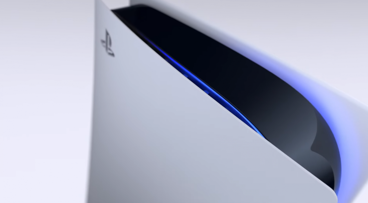
Remember the PlayStation 5 uses a single 7nm SoC from AMD outfitted with a Navi GPU and Zen 2 CPU.
The patent's main goal is to present the possibility of a multi-GPU console with both local and network access to the second GPU. So there's two main ways this could work: A physical console that contains two GPUs, whether it be two SoCs/APUs, or one SoC and a second GPU; or using a GPU from a cloud server network.
The latter is how the PlayStation Now service is powered.
When it comes to physical dual-GPU setups, the patent recognizes there's significant hurdles to tackle such as frame buffer management for rendering. The patent is extremely varied and detailed and aims to cover all the bases for a solution to this problem.
So instead of outlining every single possible solution, we'll give you the gist (we'll also include a full copy of the summary at the bottom of the article for your perusal).
Some of the embodiments have the rendered video split up between the GPUs. One GPU renders one part, the other renders the other part, and the system uses multi-plexing to combine the rendered images and output them to a screen.
(...)
PlayStation 5 Pro with multi-GPU tech outlined in new Sony patent
A new Sony patent suggests a high-end PS5 Pro console with multiple GPUs, or perhaps even a low-cost box powered by PS Now.
 www.tweaktown.com


