If you mean the Minecraft tech demo that was shown to Digital Foundry, how did you manage to take any conclusions out of that? We know that for 2070 the average framerate is around 50 fps at full hd - what is the framerate on XSX? And is the demo rendering the exact same thing that the game does on a pc?
According to Microsoft, the demo ran between 30 FPS - 60 FPS, so dead in the middle would be 45 FPS, which is the average for the RTX 2070 (
https://www.tomshardware.com/uk/features/minecraft-rtx-performance). We don't know if the workloads are exactly equivalent, and we also don't know if the XSX can get faster with more shader optimisation. As for example, denoising is a huge performance sink, and is performed on the shaders even in Nvidia hardware. (One of the big reasons Nvidia doubled up FP32 compute was to improve denoising performance)
So to be clear, this is just informed speculation. I am not claiming we know XSX is on par with the 2070 in raytracing; just that it is within the realms of possibility.
The next jump (albeit based on wild, baseless speculation) would make sense. But the last one, another 35-50% which is yet again absolutely massive, would stem simply from clockspeed improvements?
Well, it's based on the consistent rumours of Navi 21 being a 80 CU part. I am not saying we should expect a 35% to 50% clockspeed improvement. I am saying that if the XSX performs around 2070 levels for raytracing, then a 54% increase in CUs would put it at around 2080 Ti levels, where the 3070 is, according to Nvidia. And then it would be reasonable to think AMD could increase clocks by 15% or 20%.
In that situation it would still be behind the 3080 in raytracing, but ahead of the 3070. The 3070
should be doing much better than a 2080 Ti, but it looks like it is being starved by memory bandwidth as it has 17% less than the 2080 Ti, and raytracing demands huge amounts of bandwidth.
And what about more complex games that require compute units to do actual scene rendering in a traditional manner? How will that work if we already assumed that the entire die is going to be used for compute units - no ray tracing at all?
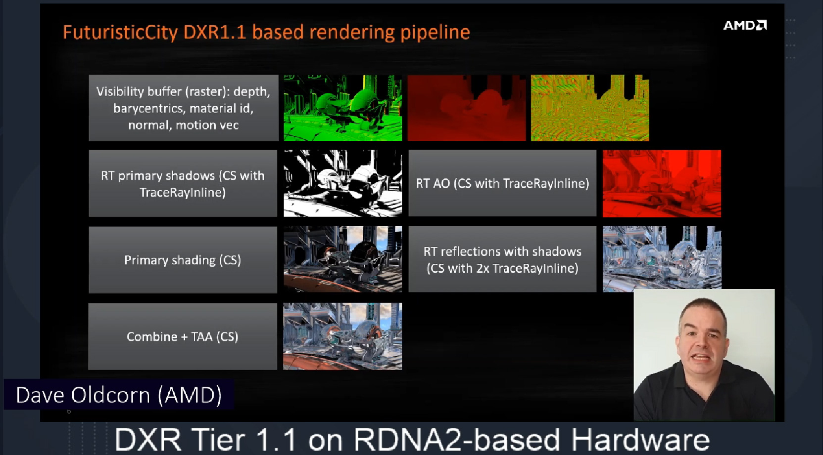
In RDNA 2, each CU contains a raytracing unit that accelerates BVH calculations, just like with Nvidia. We know from the Hot Chips presentation that this only adds a small amount of extra die space, which explains why AMD can fit 56 CUs in ~300mm^2.
As for die size, we know, that AMD was experiencing problems with smaller dies, bigger die and a more complex solution naturally means more risk of failure. You can't just scale the die up by gluing extra compute units on, you need to take things like redundancy and heat aggregation into account. Somehow, law of physics no longer apply to AMD.
AMD has been using huge dies for years. Vega 64 was 486mm^2, Fury X was 596mm^2, R9 290 was 438 mm^2. Obviously cost, heat and power consumption scale with die size, which is why AMD had to improve performance per watt by 50% with RDNA2 and why AMD will be charging more for Big Navi! But in terms of their historical "big" GPUs, 500 mm^2 is a perfectly normal die size for AMD. I find it funny that you talk about AMD breaking the laws of physics when the 3080 is 627mm^2 and the 2080 Ti was 754 mm^2!
As far as failure rates go, again card failures != silicon failures. But if you are referring to the below article, then Asrock, MSI and Sapphire all had failure rates of 2%, which is equivalent to the best AIBs on the Nvidia side. Essentially it seems that Powercolor boards were not as well built, and brought the average failure rates up.
It's marginal though. Germany based Mindfactory store revealed the number of sales and RMA of each graphics card, and Nvidia came out on top in both sales quantity and a lower percentage of graphics ...

www.guru3d.com